Monolayer Graphene on SiO2/Si Substrate, Size: 4"
- SKU:
- NG01CG0103
- UPC:
- MPN:
- Shipping:
- Calculated at Checkout
MSRP:
Now:
€423.00
Was:
— You save
Frequently bought together:
Description
1 piece/423 €
5 pieces/1864 €
Please contact us for quotes on larger quantities !!!
Monolayer Graphene on SiO2/Si Substrate
Size: 4", Grain Size: 6-10 μm
Technical Properties of Graphene Film: |
|
| Transparency | > 95 % |
| Coverage | > 93% |
| Thickness (theoretical) | 0.340 nm |
| Sheet Resistance | 500-530 Ohms/sq |
| Grain Size | 6-10 μm |
Technical Properties of SiO2/Si Substrate: |
|
| Size (inch) | 4'' |
| Dry Oxide Thickness | 300 nm |
| Type | Phosphor doped / N type |
| Orientation | <100> |
| Resistivity | 0.001 - 0.01 |
| Thickness | 525 +/- 20 μm |
| Front surface | One Side Polished |
Applications:
Graphene research; Supercapacitors; Catalyst; Solar energy; Graphene optoelectronics, plasmonics and nanophotonics;
Graphene semiconductor chips; Conductive graphene film; Graphene computer memory; Biomaterials and Bioelectronics.
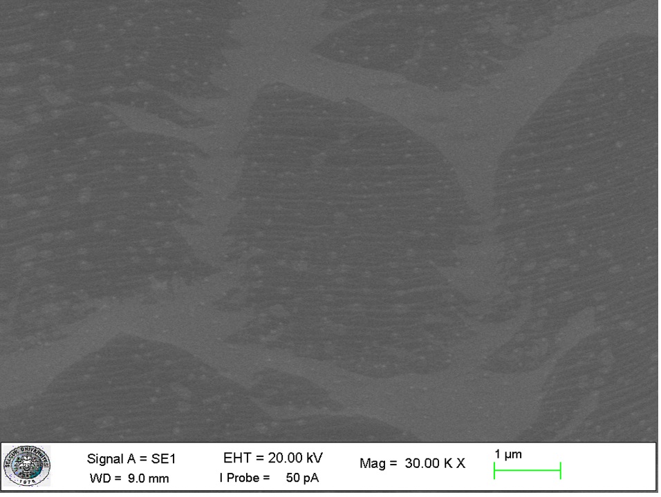
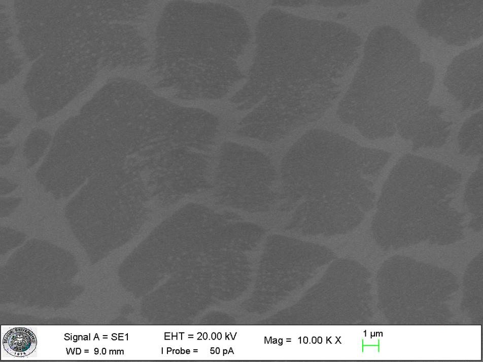
SEM Image of Monolayer Graphene
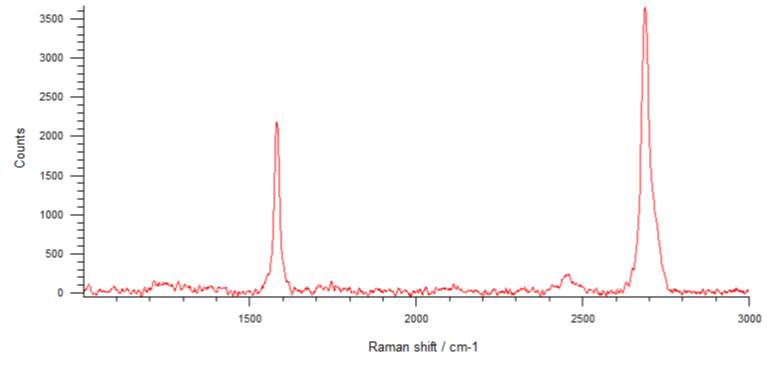
Raman Image Of Monolayer Graphene
Method of Preparation Graphene on Si/SiO2 Substrate was prepared by the following steps: |
| 1) Single layer graphene grown on copper foil |
| 2) Deposit PMMA and curing process |
| 3) Remove Cu by etching process |
| 4) Wash PMMA/Graphene in DI water |
| 5) Redeposit PMMA/Graphene onto Si substrate and curing process |
| 6) Remove PMMA with aceton |
Related Products


Graphene Nanoplatelet, Purity: 99.9+%, Size: 5 nm, S.A: 135 m2/g, Dia: 30 μm
MSRP:
Now:
€9.00
Was:
1 gram: 9 €5 grams: 17 € 25 grams: 48 € ...
NG01GNP0103
Monolayer Graphene on SiO2/Si Substrate, Size: 2"
MSRP:
Now:
€269.00
Was:
1 piece/ 269 € 5 pieces/ 1094 €
Please contact us for quotes on larger quantities !!!
Monolayer Graphene on SiO2/Si Substrate
Size: 2"
NG01CG0101

Monolayer Graphene on SiO2/Si Substrate, Size: 3"
MSRP:
Now:
€324.00
Was:
1 piece/324 €5 pieces/1369 €
Please contact us for quotes on larger quantities !!!
Monolayer Graphene on SiO2/Si Substrate
Size: 3", Grain Size: 6-10 μm
NG01CG0102

Silicon Dioxide (SiO2) Micron Powder, Size: <15 Micron, Purity: 99.9%
MSRP:
Now:
€18.00
Was:
25 grams: 18€
100 grams:35€
500 grams:81€
1000 grams: 122€
Product Information
Produ
NG10MPW1088
Silicon Dioxide(SiO2) Micron Powder, Size: -325 mesh,Purity: 99.9%
MSRP:
Now:
€16.00
Was:
25 grams: 16€100 grams:33€500 grams:79€
1000 grams: 120€
Product Information
Product Name
NG10MPW1089
Customers Also Viewed
POPULAR

Graphene Oxide, 2-5 Layer, Dia: 4,5 µm, SA: 420 m2/gr
MSRP:
Now:
€75.00
Was:
1 gram / 75 €5 grams / 269.50 € 25 grams / 742.50 € ...
NG01GO0102

Monolayer Graphene on SiO2/Si Substrate, Size: 2"
MSRP:
Now:
€269.00
Was:
1 piece/ 269 € 5 pieces/ 1094 €
Please contact us for quotes on larger quantities !!!
Monolayer Graphene on SiO2/Si Substrate
Size:...
NG01CG0101

Single Layer Graphene Oxide, Purity: 99.5 %
MSRP:
Now:
€181.00
Was:
1 gram: 181 € 5 grams: 654 € 25 grams: 1804 € ...
NG01GO0101

Monolayer Graphene on SiO2/Si Substrate, Size: 3"
MSRP:
Now:
€324.00
Was:
1 piece/324 €5 pieces/1369 €
Please contact us for quotes on larger quantities !!!
Monolayer Graphene on SiO2/Si Substrate
Size: 3", Grain Size: 6-10...
NG01CG0102
POPULAR

Reduced Graphene Oxide (rGO),Purity: 99%, S.A: 15.62 m2/g, 2-5 layers
MSRP:
Now:
€53.00
Was:
1 gram: 53 €5 grams: 105 € 25 grams: 434 € ...
NG01RGO0101
Graphene Oxide Water Dispersion, Purity: 99.5%, Black Liquid, GO: 2,0 wt%
MSRP:
Now:
€139.00
Was:
25 ml / 139 €100 ml / 429 €500 ml / 640 €1000 ml / 862 €
Please contact us for quotes on larger...
NG04EO0717

Graphene Water Dispersion, Purity: 99.5%, Black Liquid, Graphene: 1,0 wt%
MSRP:
Now:
€73.00
Was:
30 ml/73 €60 ml/104 € 120 ml/181 € ...
NG04EO0716

Silicon Dioxide (SiO2) Micron Powder, Size: <15 Micron, Purity: 99.9%
MSRP:
Now:
€18.00
Was:
25 grams: 18€
100 grams:35€
500 grams:81€
1000 grams: 122€
Product Information
Product Name
Silicon Dioxide (SiO2 ) Micron Powder...
NG10MPW1088
NEW


Boron Doped Graphene Nanopowder (B/G)
MSRP:
Now:
€269.00
Was:
1 gram: 269 €
5 grams: 1080 €
10 grams: 1765 €
Contact us for tailored quotes on larger quantities & experience exceptional solutions from our experts.
Boron Doped...
NG01SC0715

Lithium Chips for Coin Cell Materials, Diameter: 16 mm, Thickness: 0.6 mm, 1500 pieces
MSRP:
Now:
€1,118.00
Was:
1 bottle/1118 € 3 bottles/2985 €
5 bottles/4232 €
Please contact us for quotes on larger quantities !!!
Lithium Chips for Coin Cell...
NG04CO08024

